
Facilities
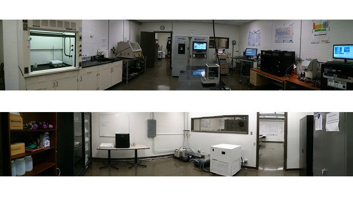
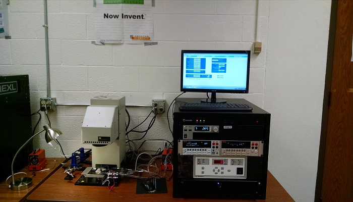
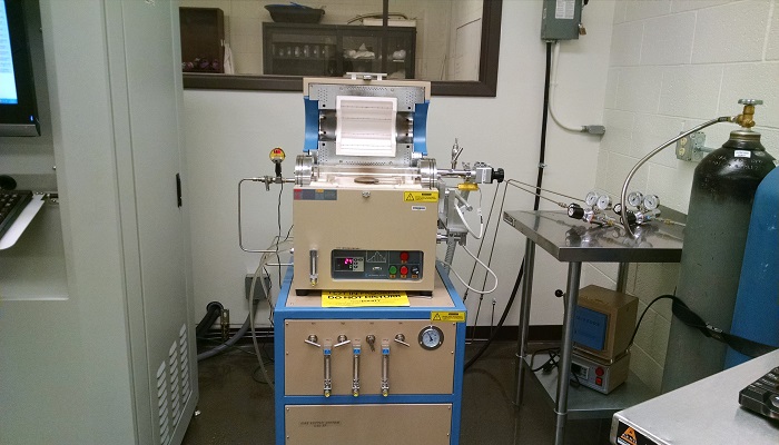
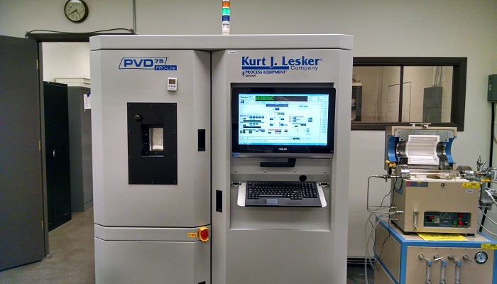
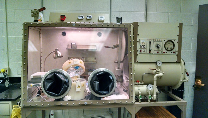
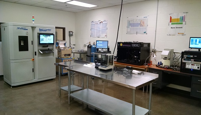
The PI has established an 846 sq. ft. laboratory facility with excellent resources to support her research of semiconductor material synthesis, device fabrication and characterization. Major equipment installed includes a sputtering and thermal evaporation system, rapid thermal furnace, spectral response system, I-V system, solar simulator, Hall Management system, Signatone 4 point probe, Keithley source meter and oscilloscope.
The PI has developed a network with Scientists and Engineers at BNL in the National Synchrotron Light Source II (NSLS II), the Center for Functional Nanomaterials (CFN), the Nonprofileration and National Security (NN) and Physics departments. The PI is a beamline user of NSLS II and a user of CFN with approved proposals. Additional tools used at BNL include the NSLS II QAS, XPD and SRX beamlines (QAS, XPD, XRF and XANES), CFN’s PL, SEM/FIB, XPS and AFM.

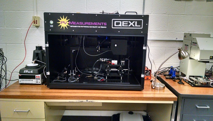
Included in the suite of fabrication and characterization tools include a Kurt J. Lesker PVD75 thin film material physical vapor deposition system, a MTI Rapid Thermal Processing System and a Muffle Furnace, a Signatone 4 point probe, a Laurell Technology Spin Coater, and a PV Measurements I-V and EQE system.